
Electropolished Tubing for Semiconductor Manufacturing: Clean & Reliable Solutions
Discover how Electropolished Tubing for Semiconductor Manufacturing enhances contamination control, ensuring ultra-clean environments and reliable performance for high-tech production processes
Sheentube
10/27/20242 min read
How Do Electropolished Tubes Prevent Contamination in Semiconductor Manufacturing?
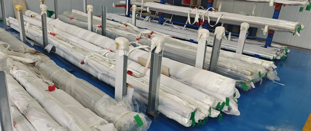
Electropolished stainless steel tubes are essential in semiconductor manufacturing, where the highest standards of cleanliness are required. The electropolishing process removes microscopic surface impurities, resulting in ultra-smooth, highly reflective tubing. This smooth surface limits contaminant accumulation and prevents particle shedding, ensuring an environment suitable for semiconductor processes.
What is Electropolishing and Why is it Important?
Electropolishing is an electrochemical process that strips away microscopic surface layers of metal, polishing the tube to an exceptional smoothness. Unlike mechanical polishing, which may leave micro-grooves or abrasions, electropolishing results in a homogenous and reflective finish. In semiconductor manufacturing, this smooth finish is critical for two reasons:
Reduced Particulate Contamination: Microgrooves on tubing surfaces can harbor particulates that are dislodged during the production process. Electropolished tubes eliminate these potential traps, reducing particulate contamination risks.
Increased Corrosion Resistance: The process creates a layer rich in chromium oxide, increasing corrosion resistance, especially against chemical agents commonly used in semiconductor manufacturing.
The Role of Electropolished Tubing in Cleanroom Environments
Cleanrooms in semiconductor manufacturing require rigorous cleanliness. Electropolished tubing provides ultra-smooth channels, ensuring that airflow and fluid movement don’t agitate or release unwanted particles. This smoothness helps prevent the build-up of organic contaminants, crucial in maintaining air and fluid purity within cleanroom environments.
Key Benefits of Electropolished Tubes in Semiconductor Applications
Electropolished tubes offer distinct advantages in the semiconductor sector:
Surface Purity: With surface roughness often below 0.25 microns, electropolished tubes have minimal particle adherence.
Enhanced Durability: The chromium-rich oxide layer increases durability against harsh chemicals used in etching and cleaning processes.
Better Fluid Dynamics: Smooth tubing surfaces reduce fluid resistance, enhancing overall system efficiency and reducing turbulence that can lead to contamination.
Meeting SEMI F19 Standards
Electropolished tubing meets SEMI F19 standards, which specify surface roughness and other properties crucial to semiconductor manufacturing. Meeting these standards means that electropolished tubing aligns with industry expectations, supporting manufacturers in achieving quality and compliance.
Conclusion
For semiconductor manufacturing, maintaining cleanliness and purity is essential. Electropolished stainless steel tubing is a key component in minimizing contamination, enhancing corrosion resistance, and supporting efficiency in cleanroom environments. This tubing provides not only the physical purity needed but also the performance and reliability that semiconductor facilities demand, contributing to the production of quality semiconductor components.

Sheentube
High-quality stainless steel tubes for industries.
+86 15203012590
© 2024. All rights reserved.